315-5345: Difference between revisions
Jump to navigation
Jump to search
(Created page with "right|thumb == 315-5345 == The 315-5345 is a clock divider. It takes the MCLK signal and generate the VCLK (for the M68K) and the ZCLK (for the Z80). ...") |
|||
| (4 intermediate revisions by one other user not shown) | |||
| Line 3: | Line 3: | ||
== 315-5345 == | == 315-5345 == | ||
The 315-5345 is | The 315-5345 is found in the Model 1 Genesis VA2 revision and in the Megatech arcade system. | ||
== Pinout == | |||
[[File:315-5345_pinout.png|600px]] | |||
[[ | The /BGACK pin is connected to the one of the [[315-5313]], not the /BGACK pin of the 68000. | ||
OpenOffice Draw file : [[File:315-5345.odg]] | OpenOffice Draw file : [[File:315-5345.odg]] | ||
Latest revision as of 18:23, 9 February 2013

315-5345
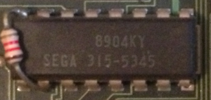
The 315-5345 is found in the Model 1 Genesis VA2 revision and in the Megatech arcade system.
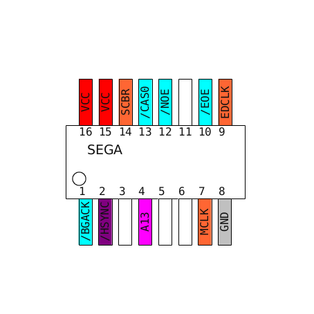
Pinout
The /BGACK pin is connected to the one of the 315-5313, not the /BGACK pin of the 68000.
OpenOffice Draw file : File:315-5345.odg
Signal
| Address Buses | |
| A1-A23 | M68K Address Bus |
| ZA0-ZA15 | Z80 Address bus |
| Data Buses | |
| D0-D15 | M68K Data bus |
| ZD0-ZD7 | Z80 Data bus |
| IO port lines | |
| EM1X | Port 1 lines |
| EM2X | Port 2 lines |
| EM3X | Port 3 lines |
| Control lines | |
| M68K related control lines | |
| /BG | Bus Grant |
| /BGACK | Bus Grand Acknowledge |
| /BR | Bus Request |
| FC0 | Function Code 0, 1 = Accessing user data |
| FC1 | Function Code 1, 1 = Accessing user program |
| /HALT | Halt 68K execution |
| /RESET | Reset 68K |
| /VPA | Valid Peripheral Access |
| /AS | Address strobe |
| /DTACK | Data Acknowledge |
| /UDS | Accessing even bytes |
| /LDS | Accessing odd bytes |
| R/W | Read/Write pin, 0 = write 1 = read |
| Z80 related control lines | |
| /ZM1 | Opcode fetch strobe |
| /ZRD | Read strobe |
| /ZWR | Write strobe |
| /ZMREQ | Memory request |
| /ZIORQ | IO request |
| /ZNMI | Non-maskable IRQ |
| /ZBR | Bus request |
| /ZBAK | Bus Acknowledge |
| /ZRES | Reset Z80 |
| /ZWAIT | Wait |
| Address decoding related control lines | |
| /ASEL | Read or Write on $000000-$7FFFFF region |
| /CAS0 | Read or Write on $000000-$DFFFFF region |
| /RAS0 | Read or Write on $E00000-$FFFFFF region, act as /CE signal for the RAM chips |
| /CE0 | Chip Enable for the cartridge, low when accessing $000000-$3FFFFF region when expension unit isn't inserted or $400000-$7FFFFF when it is. |
| /TIME | Read or Write on $A13000-$A130FF region |
| /LWR | Lower byte WRite |
| /UWR | Upper byte WRite |
| /NOE | /OE signal for the lower part of the RAM |
| /EOE | /OE signal for the upper part of the RAM |
| /ZREF | Unknown, tied to unused pin #1 of Z80 RAM |
| /ZRAM | /CE for the Z80 RAM |
| Configuration related control lines | |
| /DISK | 0V Expansion Unit connected |
| FREQ | 5V = 60Hz, 0V = 50Hz |
| /FRES | |
| LANG | 5V = English, 0V = Japanese |
| /M3 | Mark III compatibility mode |
| VRAM related control lines | |
| /CAS1 | Column address strobe |
| /RAS1 | Row address strobe |
| /SE0 | Serial data bus /OE |
| SC | Serial clock |
| /WE0 | Write enable |
| /OE1 | Output enable |
| Clock lines | |
| MCLK | Master Clock |
| VCLK | 68K clock |
| ZCLK | Z80 clock |
| EDCLK | Unknown clock |
